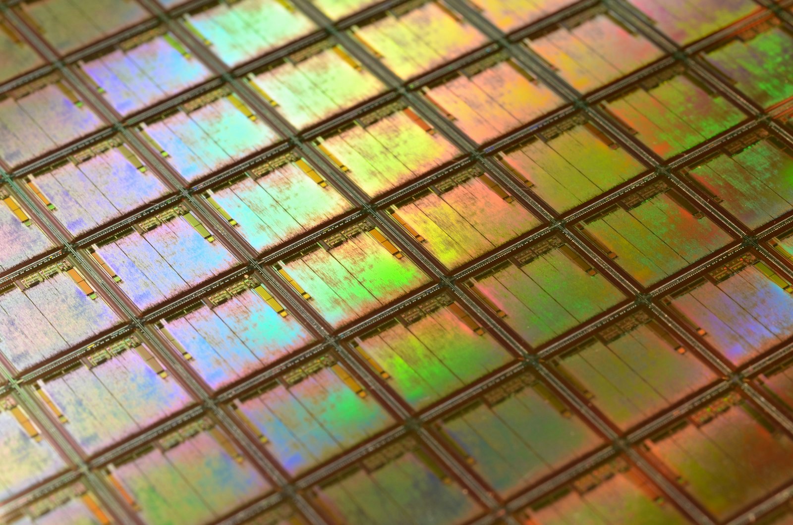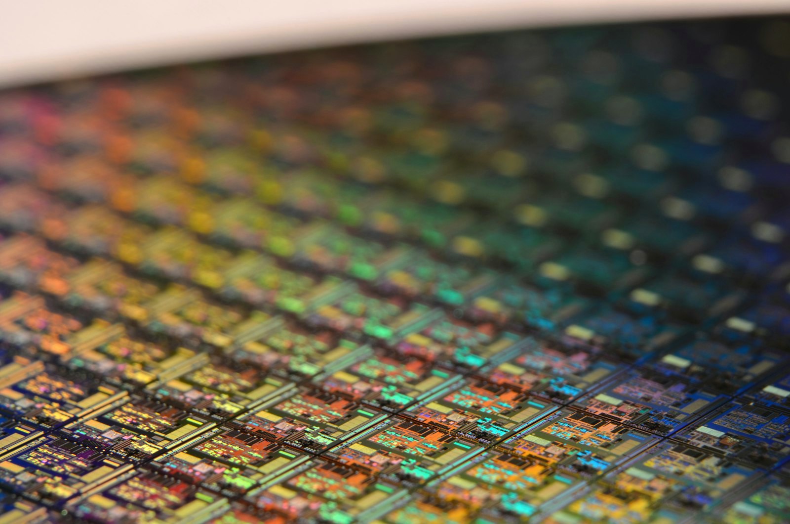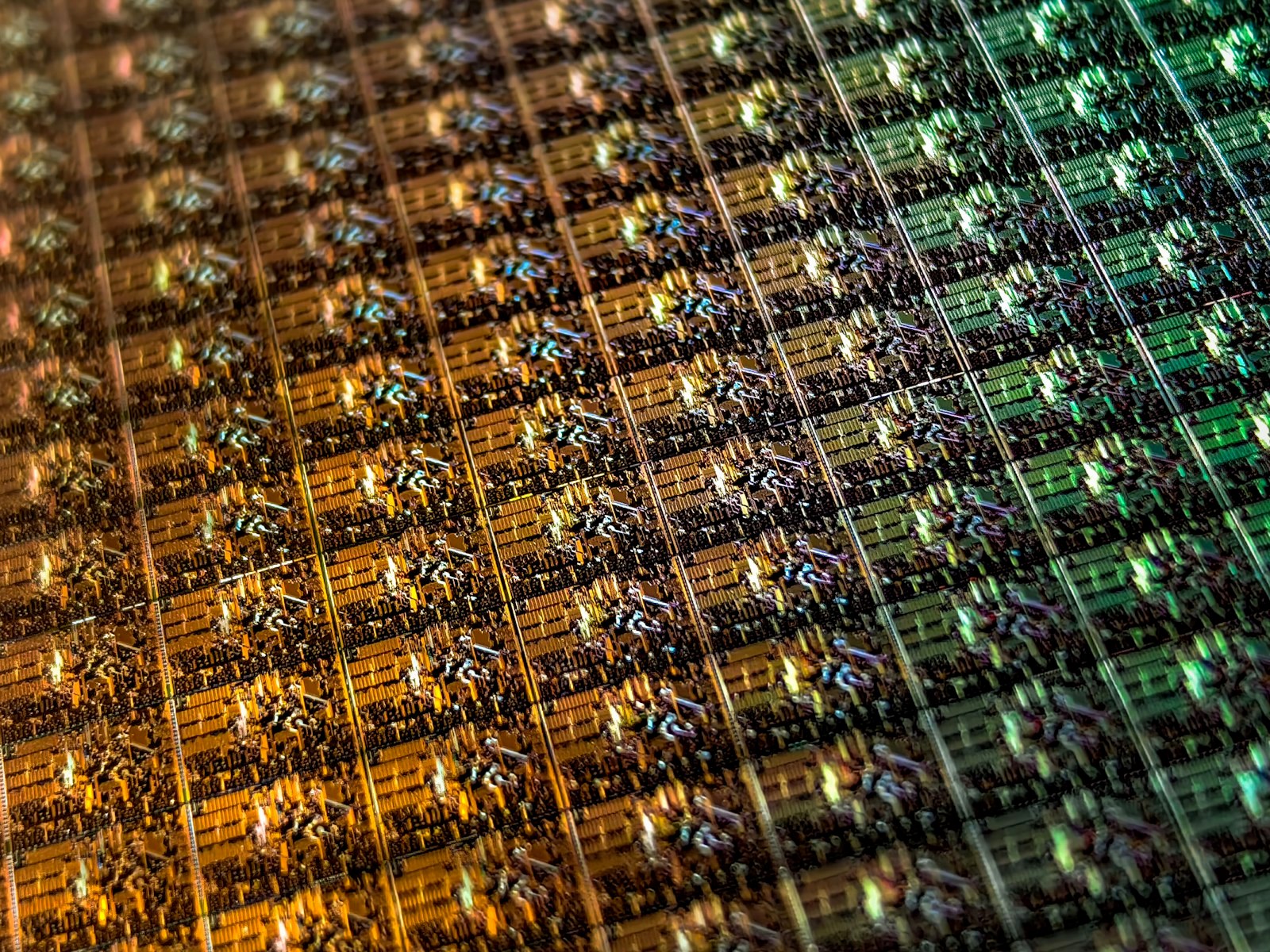
Imagine shrinking yourself down to a few nanometers and stepping onto a silicon wafer. Instead of just seeing a sterile grid of transistors and wires, you suddenly stumble upon a tiny portrait, a whimsical animal, or a cryptic message. Welcome to the world of chip art—the hidden, microscopic graffiti of the semiconductor industry.
Silicon Doodles
Chip art, also known as silicon doodling, refers to the intentional placement of non-functional drawings and symbols within the layers of an integrated circuit (IC). Because chips are produced using photolithography—essentially printing a complex map of the circuit—engineers can add these artistic flourishes without adding any extra cost to the manufacturing process. As long as the art doesn't interfere with the electrical paths, it's essentially 'free' real estate.
Why Do Engineers Do It?
For the designers, it's a mix of tradition, branding, and sheer boredom. Some artists use these spaces to leave a digital signature, while others create elaborate landscapes or characters as a secret easter egg for anyone curious enough to examine the chip under a powerful microscope. It transforms a piece of cold, industrial hardware into a canvas for human expression, proving that even in the most rigid technical environments, creativity finds a way to leak through.
As we move toward an era of increasingly automated design and AI-generated layouts, one has to wonder: will the tradition of the human 'silicon doodle' survive, or will the art of the chip become a relic of the past?
Sources
Media